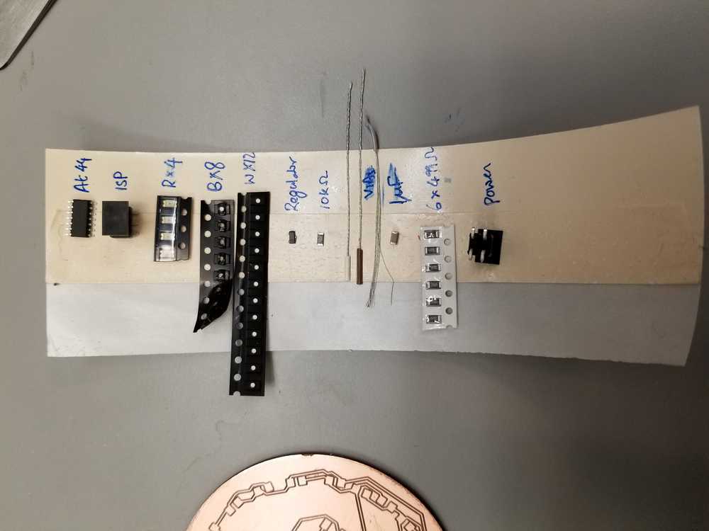
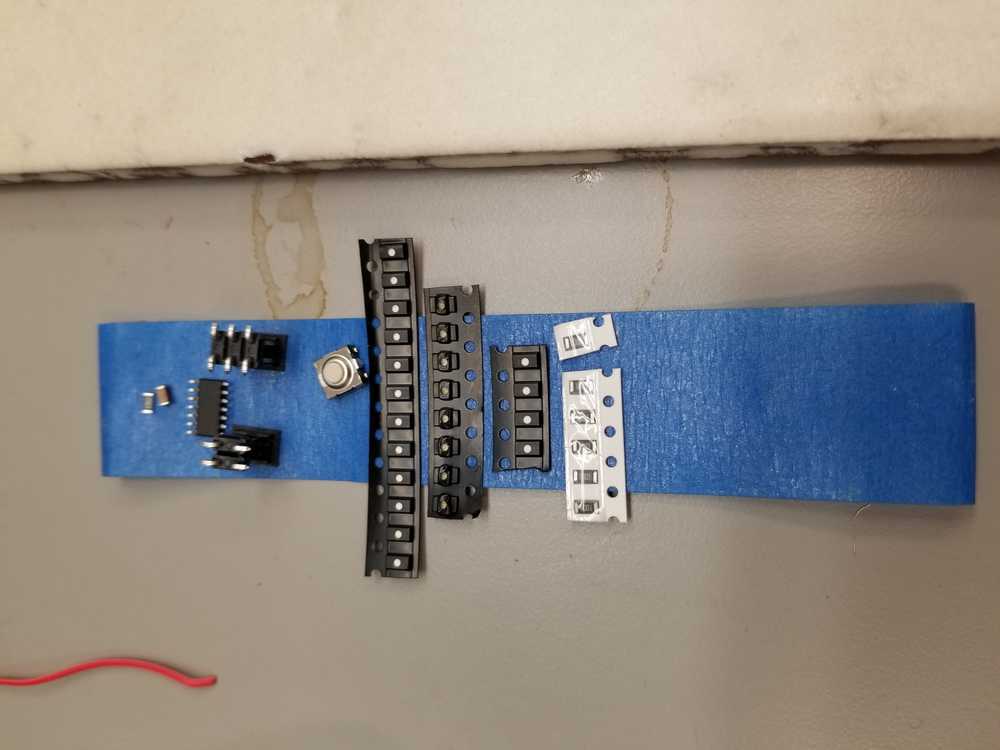
Designing the board
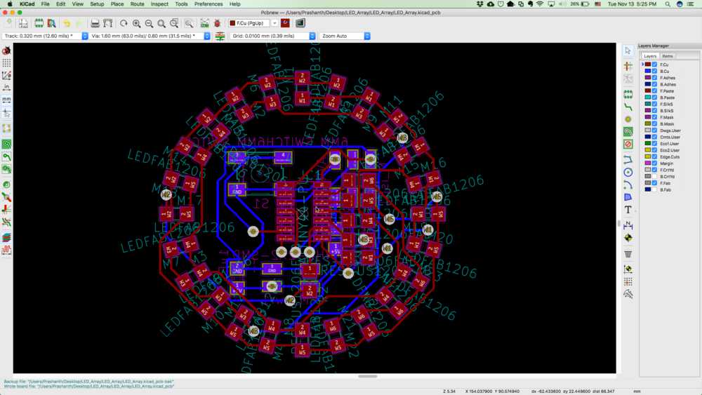
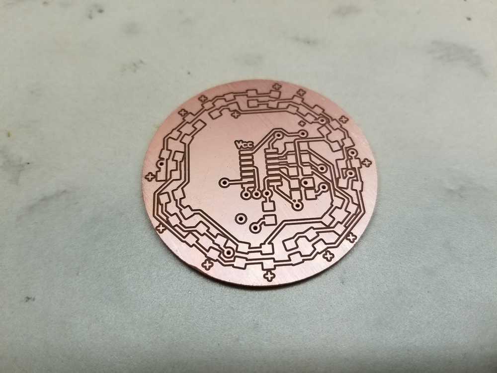
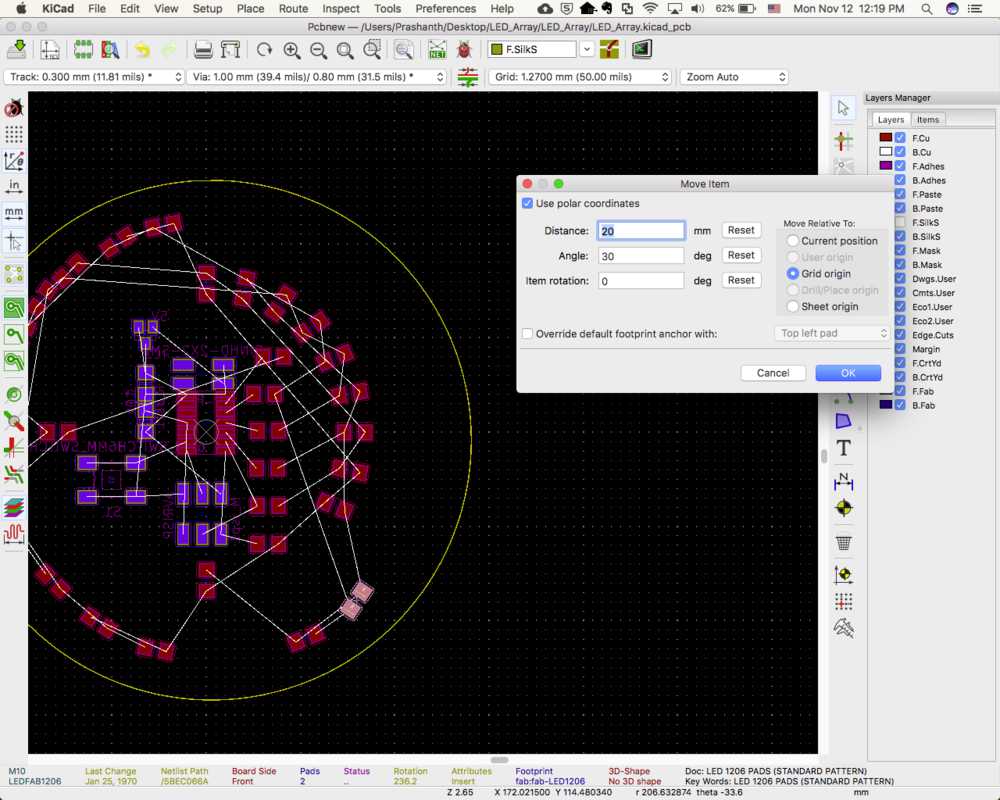
I decided to use this week to practice/prototype for my final project - a somehwat-smart watch. The picture to the left here shows the final PCB layout that I converged upon. As you can see this "digitally powered analog clock face" is still missing some components that I want to add such as a accelerometer, a bluetooth module, a thermistor and maybe a GPS module.
 I think it was a good idea to do this practice run, I came across several issues that I will need to still solve for my final project.
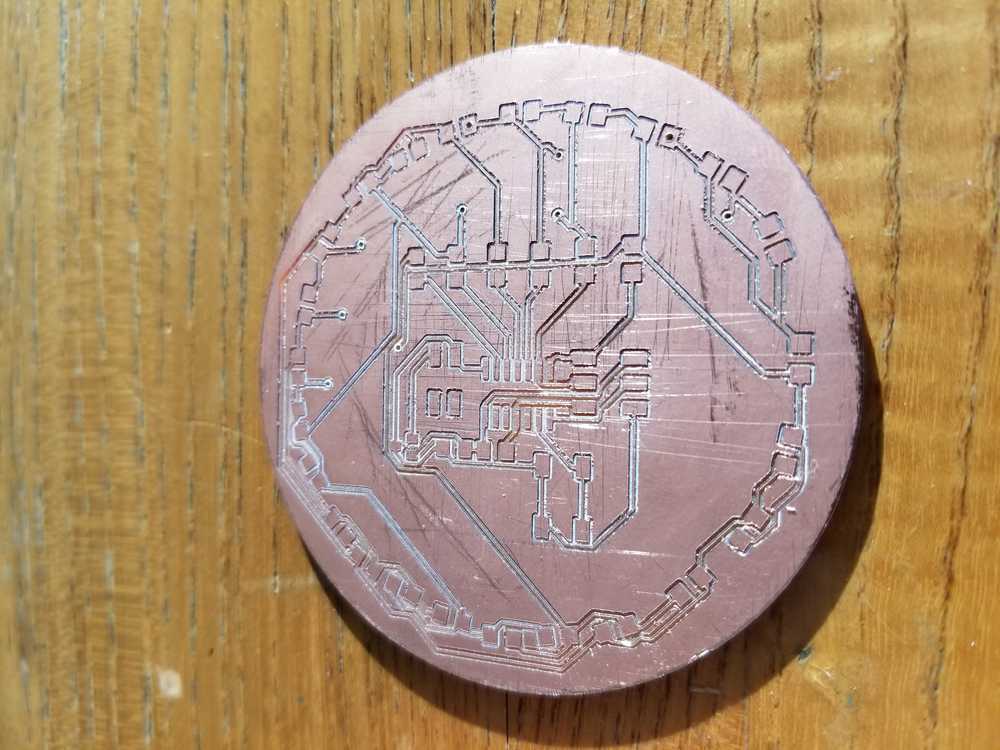
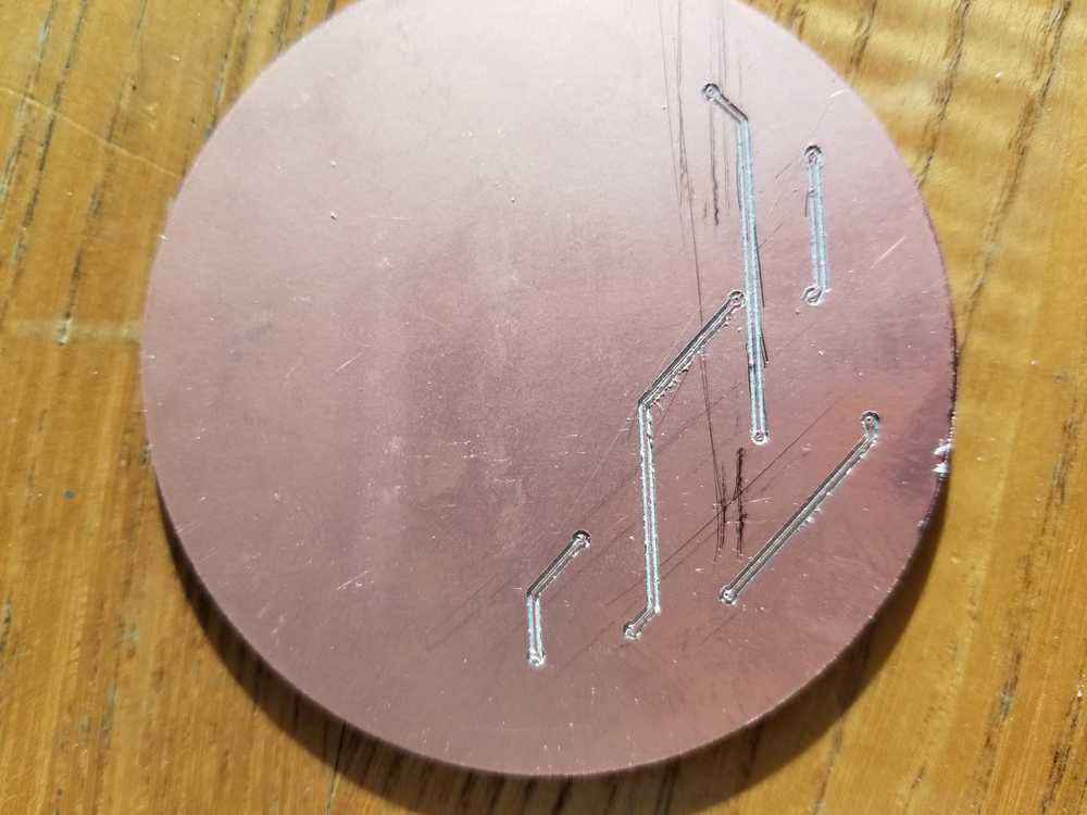
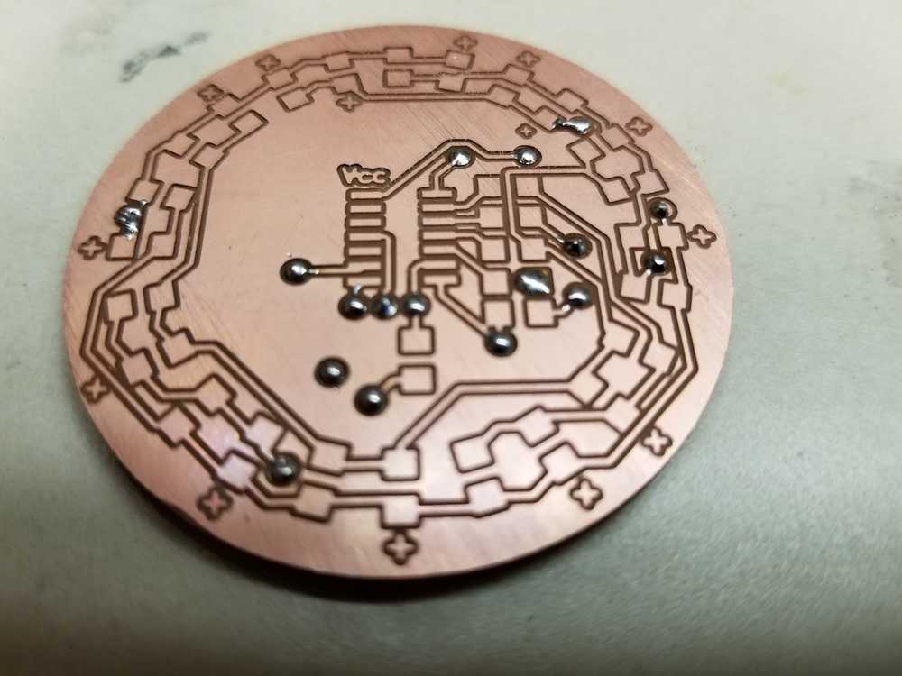
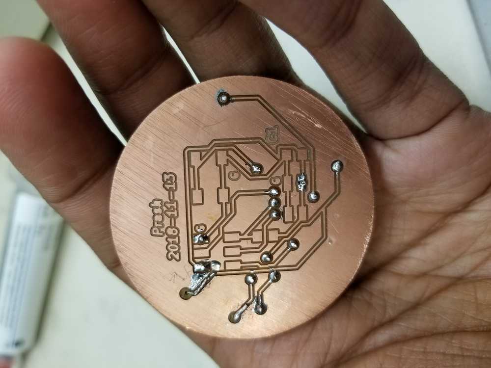
Considering the small form factor that I want, I almost certainly need to use both sides of the board. We still don't have rivets so I'm using the through wire + solder method. It seems to work ok, except sometimes while adding other components close to the vias, the solder gets hot enough that the wire core is displaced resulting in a poor connection.
I think it was a good idea to do this practice run, I came across several issues that I will need to still solve for my final project.
Considering the small form factor that I want, I almost certainly need to use both sides of the board. We still don't have rivets so I'm using the through wire + solder method. It seems to work ok, except sometimes while adding other components close to the vias, the solder gets hot enough that the wire core is displaced resulting in a poor connection.
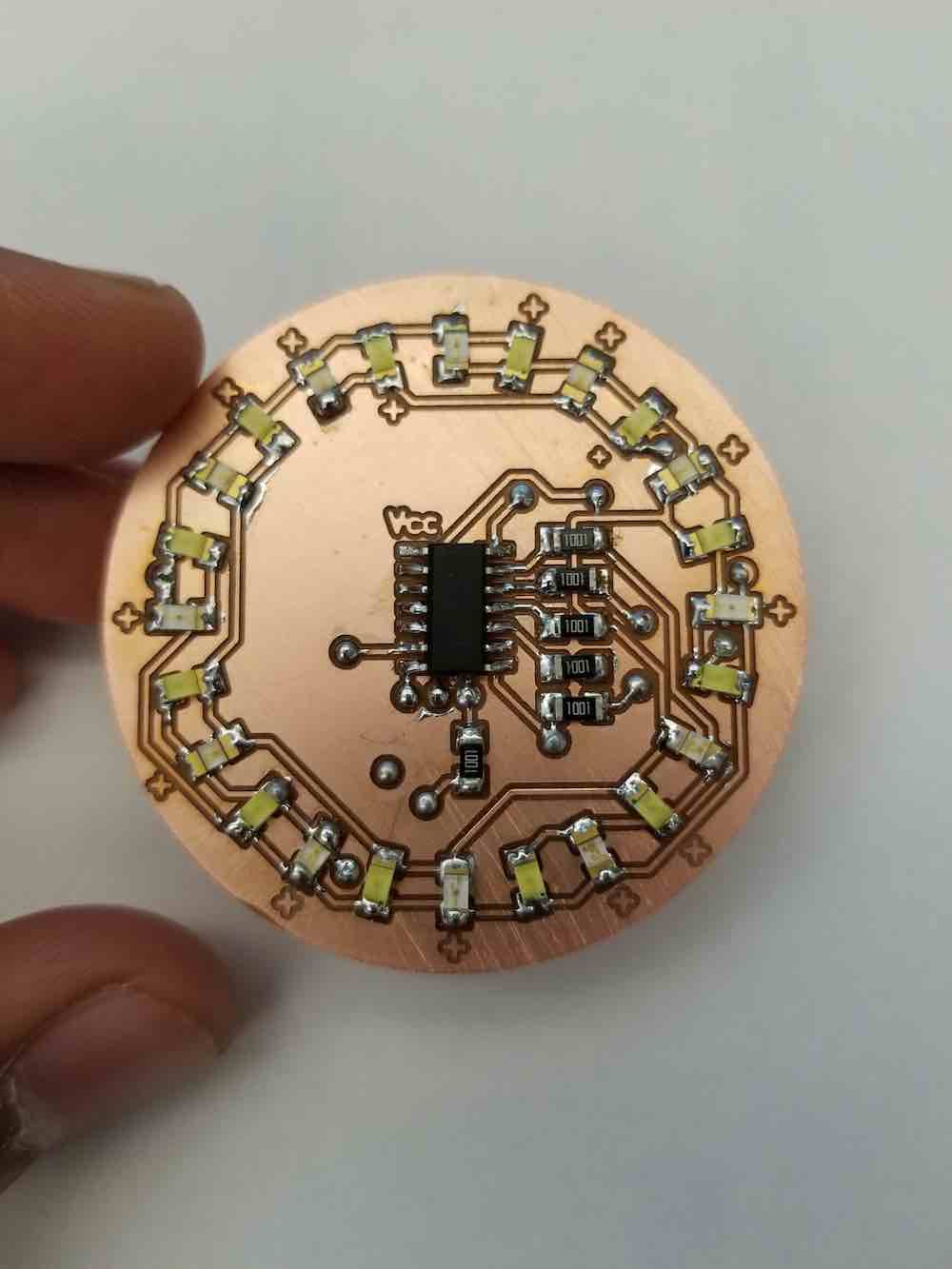
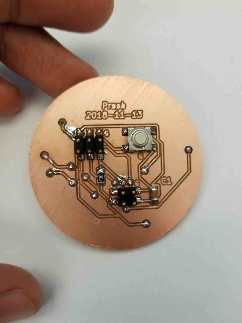
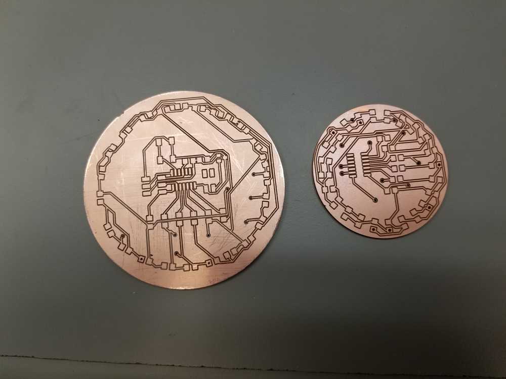
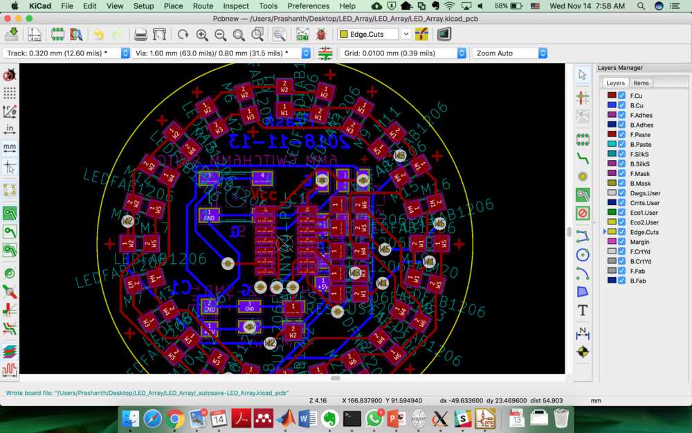
The following pictures show the different iterations where the PCB size got smaller, the positioning of the LED's became more precise and I started adding labels on the copper itself to speed up the soldering and populating process.
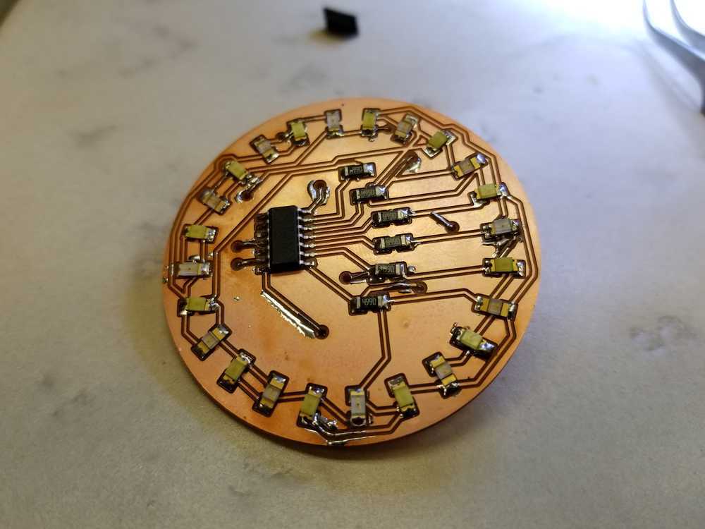
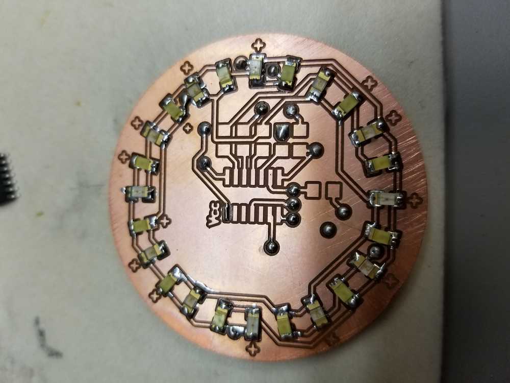
There are still clearly some issues, some of the LED's don't seem to light up as expected. I checked the pin outputs form the attiny using the oscilloscope, they seem to be doing something. I resoldered a couple of LEDs and then they started workign. I suspect poor joints especially in the vias. I'm still looking into this at the moment.